A SiC MOSFET fails at 900 volts. Its datasheet rating is 1200 volts. The gate drive is correct. The thermal management is adequate. The schematic is, as always, innocent. The failure trace leads not to a component but to a geometric property of the copper — a property that has no symbol in the schematic, appears in no BOM line, and is invisible until the device destroys itself on the first switching edge at full voltage.
That property is parasitic loop inductance. And in a SiC circuit, it is not a secondary consideration. It is the design.
The previous post in this series identified parasitic loop inductance as the dominant enemy in power converter PCB design — the fight that makes a power conversion board fundamentally different from an EV charger board or a BMS board. This post goes inside that enemy. What it is. Where it lives. What it does to a SiC device. And what the layout must do about it.
What Is Parasitic Loop Inductance?
Every current-carrying conductor has inductance. This is not a design defect — it is a fundamental property of electromagnetism. When current flows through a conductor and changes with time, the inductance of that conductor resists the change by inducing a voltage. The faster the current changes, the larger the induced voltage.
In a power electronics PCB, the current does not flow through a single conductor. It flows through a loop — from the DC bus capacitor, through the top switch, through the load or transformer, through the bottom switch, and back to the capacitor. Every segment of copper in that loop contributes inductance. The sum of those contributions is the parasitic loop inductance of the commutation loop.
It is called parasitic because it was not designed into the circuit. No engineer placed an inductor symbol on the schematic. But the inductance is real, it is present in every PCB, and it cannot be avoided — it can only be managed through the geometry of the layout.
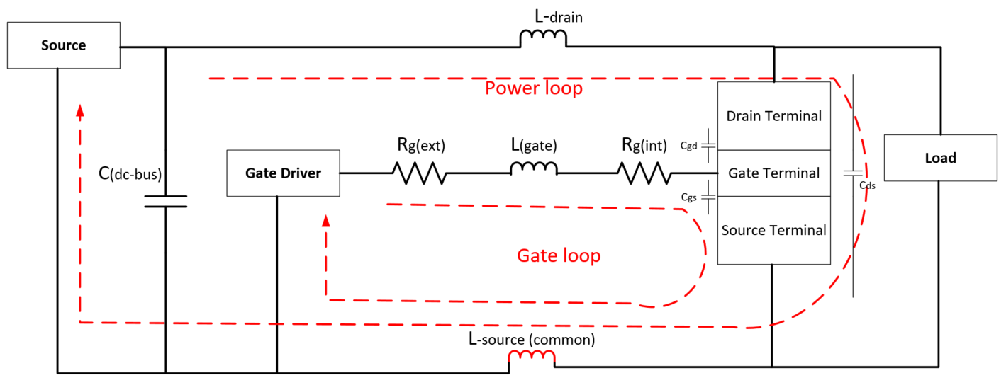
Figure 1 — The commutation loop
Every copper segment contributes partial inductance. The total loop inductance is the sum of all contributions — L_trace, L_package, L_cap_ESL, and L_common_source.
The Power Loop and the Gate Loop — Two Different Fights
Power electronics PCB designers must manage two distinct inductive loops, each with its own failure mode.
The power loop carries the commutation current — the current that switches between the top and bottom devices on every switching cycle. Its inductance produces voltage overshoot on the drain of the switching device during turn-off. This overshoot adds directly to the bus voltage and can push the device beyond its rated breakdown voltage.
The gate loop carries the gate drive signal — the current that charges and discharges the gate capacitance during switching. Its inductance, particularly in the section shared with the power loop at the MOSFET source (the common source inductance), induces a voltage that opposes turn-on and can cause false triggering during turn-off. This is a subtler failure mode but equally destructive over time.
Both loops must be managed. The power loop inductance determines overvoltage risk. The gate loop inductance determines switching speed and false turn-on risk. They share one critical node — the MOSFET source — which is why the common source inductance is the most overlooked and most consequential parasitic in a SiC gate drive layout.
Why It Matters More for SiC Than for Silicon
Silicon IGBTs switch in microseconds. SiC MOSFETs switch in nanoseconds. At the same bus voltage and load current, a SiC device switches ten to fifty times faster than a silicon device. That speed advantage is why SiC exists — lower switching losses, higher frequency operation, smaller magnetics.
But the same speed that reduces switching losses also amplifies the consequences of parasitic inductance. The governing equation is direct and unforgiving:
V = L × dI/dt The voltage spike induced by a parasitic inductance is proportional to the inductance and to the rate of current change. |
In a silicon IGBT circuit switching at dI/dt = 1 A/ns through 30 nH of loop inductance, the induced voltage spike is 30 V — manageable headroom for a 1200 V device.
In a SiC MOSFET circuit switching at dI/dt = 10 A/ns through the same 30 nH, the induced spike is 300 V — added directly to the bus voltage. On an 800 V bus, the device now sees 1100 V. A 1200 V rated device has a 20% derating recommendation, placing its safe operating limit at 960 V. At 1100 V, the device is 140 V above its derated limit on every turn-off event.
The inductance did not change. The device rating did not change. The bus voltage did not change. Only the switching speed changed — and that change transformed a manageable parasitic into a device-destroying voltage source.
What Parasitic Inductance Looks Like in a Real Design
The consequences of excessive loop inductance in a SiC circuit present in three forms, each progressively more severe.
Voltage Overshoot at Turn-Off
At the moment a SiC MOSFET turns off, the current that was flowing through it must rapidly transfer to the freewheeling path. The parasitic inductance of the commutation loop resists this transfer — by generating a voltage spike on the drain of the switching device that adds to the bus voltage. The spike decays as the energy stored in the inductance is dissipated through resistive losses and the device's output capacitance.
This overshoot is repeatable and predictable. The peak drain-source voltage at turn-off is:
Vds_peak = Vbus + Z0 × IL where Z0 = √(L_loop / Coss) is the characteristic impedance of the LC tank formed by the loop inductance and the device output capacitance, and IL is the load current at the moment of turn-off. |
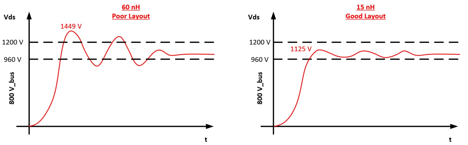
The following table shows the calculated result for a 1200 V SiC MOSFET at 800 V bus voltage and 25 A load current under two layout scenarios — a good layout with 15 nH loop inductance and a poor layout with 60 nH. These are real numbers, calculated from the device datasheet parameters of a commercial 1200 V SiC MOSFET (Coss = 89 pF at 800 V):
| Parameter | Good Layout (15 nH) | Poor Layout (60 nH) |
|---|---|---|
| Ringing frequency f_ring | 138 MHz | 69 MHz |
| Characteristic impedance Z0 | 12.98 Ω | 25.96 Ω |
| Peak overvoltage ΔV_peak | 324 V | 649 V |
| Vds_peak at 800 V bus | 1,125 V | 1,449 V |
| 20% derated limit (1200 V device) | PASS — within 960 V limit? No — 165 V over | FAIL — 489 V over limit |
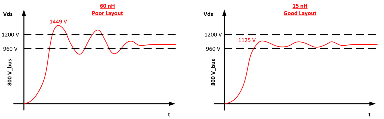
Figure 2 — Simulated Vds turn-off waveforms for L_loop
L_loop = 60 nH (poor layout, left) and L_loop = 15 nH (good layout, right). Bus voltage: 800 V, load current: 25 A, device: 1200 V SiC MOSFET. The dashed lines mark the device voltage rating (1200 V) and the recommended 20% derated operating limit (960 V). At 60 nH, the first overshoot peak reaches 1449 V — 489 V above the derated limit on every turn-off event.
At 60 nH — a loop inductance that is not unusual in a carelessly laid out SiC half bridge — the device sees 1449 V on every turn-off event. A device rated at 1200 V with a recommended 20% derating sees 489 V of margin violation on every switching cycle. The device will fail. The only question is how many switching cycles it survives before it does.
The good layout scenario at 15 nH appears safer at first glance — 1125 V versus the 1200 V rating. But the derated operating limit is 960 V, placing even the good layout 165 V above the recommended safe operating voltage. This is the uncomfortable truth that the equation reveals: loop inductance management is not optional for SiC at 800 V bus. It is the primary design constraint.
Ringing on the Switching Node
The voltage spike at turn-off does not arrive and leave cleanly. The parasitic inductance and the device output capacitance form an LC tank circuit that rings — oscillating at the resonant frequency determined by their product. The switching node voltage overshoots, undershoots, and rings until the energy is dissipated.
At 138 MHz for the good layout scenario and 69 MHz for the poor layout, these oscillations are in the RF frequency range. They radiate from the commutation loop as the loop acts as an antenna. They couple into nearby gate traces, sensor circuits, and communication lines. They appear as interference on every oscilloscope measurement taken anywhere near the switching node. They fail EMC tests before the device thermal design is ever reviewed.
Ringing is not merely a performance problem. It is a measurement problem.
An engineer trying to characterize a SiC design on the bench will find the ringing on the drain waveform indistinguishable from genuine switching behavior — until the probe ground connection is shortened and the true waveform emerges. Measuring SiC switching nodes requires a ground barrel spring on the probe tip, the tip placed as close as possible to the drain terminal, with oscilloscope bandwidth set to at least 200 MHz.
Device Failure Mechanisms
Persistent overvoltage above the rated Vds leads to two distinct failure mechanisms, each operating on a different timescale.
Avalanche breakdown occurs immediately when Vds_peak exceeds the device's avalanche rating. The device enters avalanche conduction, dissipating the energy stored in the inductor as heat in the silicon carbide. If the energy exceeds the single-pulse avalanche energy rating, the device fails catastrophically on that switching event. If it is below the rating, the device survives the event but accumulates damage with each repetition.
Gate oxide stress is the slower, more insidious mechanism. Every voltage overshoot on the drain couples partially to the gate through the gate-drain capacitance Cgd. At SiC switching speeds with dV/dt of 20–40 V/ns, the injected gate voltage can approach the gate oxide breakdown threshold over thousands of switching cycles. The device appears to function correctly until it does not — failing at a lower voltage or a lower temperature than specification after accumulated gate oxide degradation.
Where Parasitic Inductance Hides in Your PCB
The total commutation loop inductance is the sum of contributions from every element in the current path. Understanding each contributor is the first step toward managing the total.
| Inductance Source | Typical Value | Primary Cause |
|---|---|---|
| Power loop trace inductance | 10–30 nH | Trace length, narrow width, wide loop area |
| Component package inductance | 3–7 nH | Bond wire, lead frame geometry (TO-247, TO-263) |
| Via inductance | 0.5–2 nH per via | Via length, diameter — reduced by via arrays |
| DC bus capacitor ESL | 2–5 nH | Capacitor type, lead length, placement distance |
| Common source inductance | 1–7 nH | Shared gate/power return path at MOSFET source |
The power loop trace inductance dominates in most layouts. It is determined by the length of the current path and — critically — the area enclosed by that path. A wide, short trace has lower inductance than a long, narrow trace of the same cross-section, because the current forward and return paths are closer together and their magnetic fields cancel more effectively. This is why power electronics layout guidance emphasizes broad, short polygons over conventional traces for the commutation loop.
Component package inductance is fixed by the device package choice. A TO-247 through-hole package contributes approximately 5–7 nH from its lead frame geometry. A TO-263-7 SMT package contributes 2–4 nH. Moving from through-hole to SMT for the SiC devices is one of the highest-impact single changes available in a layout redesign — not because the copper changes but because the package inductance drops by 50%.
Common source inductance deserves separate attention. The MOSFET source carries both the power current and the gate drive return current. Any inductance in this shared path appears in both the power loop and the gate loop simultaneously — amplifying its effect on switching performance and false turn-on risk. A 3 nH common source inductance without a Kelvin source pin can push the gate false turn-on risk ratio above 85%, placing the design at the edge of a red warning condition. The Kelvin source pin — provided on most modern SiC MOSFETs in multi-pin packages — eliminates this coupling by providing a separate, dedicated gate return path.
What the Layout Must Do About It
Parasitic loop inductance cannot be designed out. It can only be reduced, managed, and accepted as a first-order design constraint rather than an afterthought. Four layout strategies address it directly.
Minimize the Commutation Loop Area
The magnetic flux enclosed by the commutation loop is the root source of inductance. Reduce the enclosed area and you reduce the inductance. This means placing the positive bus copper and the negative bus copper as close together as the voltage clearance requirements permit, with the minimum possible trace length between the DC bus capacitor, the top device, and the bottom device.
Broad polygons rather than conventional traces reduce the partial inductance of each segment. The current spreads across the full width of the polygon, reducing the effective inductance per unit length. On a four-layer board with 4 oz copper, the main bus polygons should be as wide as the layout permits — limited by component placement and clearance requirements, not by convention.
The adjacent return layer strategy doubles the inductance reduction. When the positive bus copper on the top layer runs directly above the negative bus return copper on an adjacent inner layer, the magnetic fields from the two opposing current flows cancel. The effective loop inductance of the pair is a fraction of what either conductor produces alone. This is why a four-layer stack with power copper on Layer 1 and a continuous ground plane on Layer 2 produces dramatically lower commutation loop inductance than a two-layer board with the same polygon widths.
Place Decoupling Capacitors Across the Switching Loop
The decoupling capacitors placed across each switching leg — from the drain of the top device to the source of the bottom device — close the high-frequency commutation loop locally. During each switching event, the commutation current does not need to travel back to the bulk DC bus capacitor. It circulates through the local decoupling capacitor, whose inductance is only the ESL of the capacitor itself plus the inductance of the short copper connection between it and the device pads.
Placement is decisive. A decoupling capacitor placed at the output terminal rather than directly across the switching leg forces the commutation current to travel the full distance from the switching node to the capacitor and back on every switching cycle. Even 10–15 mm of additional copper adds 3–5 nH to the effective loop inductance seen by the high-frequency switching current.
Ceramic capacitors in small SMT packages (0805, 1206, 2220) with C0G dielectric minimizse the capacitor's own ESL. Film capacitors, despite their other advantages, have higher ESL and are less effective as local high-frequency decoupling elements across a SiC switching leg.
Via Matrix Optimization
In a multilayer board, the commutation current must transition between layers through vias. A single via has an inductance of approximately 0.5–1 nH depending on its diameter and the board thickness it traverses. When the power loop current must pass through even one via in each direction, the via pair contributes 1–2 nH to the loop inductance.
The solution is a via matrix — an array of multiple vias in parallel, sharing the current across many paths simultaneously. Twenty-five vias in a 5×5 grid at 1 mm spacing, each 0.3 mm diameter through a 2.35 mm board, reduces the via pair inductance to a fraction of a nanohenry. The thermal benefit is equally significant — the via matrix carries heat from the device drain tab through the board to the bottom copper pour, lowering junction temperature.
Gate Resistance and the Switching Speed Trade-off
The gate resistor controls how fast the gate capacitance charges and discharges. A lower gate resistance allows faster switching — which means higher dI/dt, which means higher V = L × dI/dt voltage spikes for any given loop inductance. A higher gate resistance slows switching — which reduces the voltage spike but increases switching losses.
This trade-off does not have a universal optimum. It is specific to the device parameters, the layout inductance, the bus voltage, and the operating current. The gate resistor must be sized to produce switching speed that keeps Vds_peak within the derated operating voltage, with sufficient margin to account for device-to-device parameter variation and thermal effects on switching speed.
Separate turn-on and turn-off resistors are standard practice in SiC gate drive design — the turn-on resistor controls the dV/dt during the switching transition (affecting EMI and voltage overshoot), while the turn-off resistor can be lower to speed up turn-off and reduce conduction loss during the transition.
The Geometry Is the Design
Parasitic loop inductance is not a component failure. It is not a material defect. It is a geometric property of the current path that the PCB layout defines. The schematic cannot show it. The simulation may underestimate it. The oscilloscope will reveal it — on the bench, at operating voltage, during bring-up — at the worst possible moment.
The Governing Observation In a SiC power converter, the layout does not carry power. It manages energy — the energy stored in every picohenry of loop inductance on every switching edge. Get the geometry right and the device operates within its ratings for its rated lifetime. Get it wrong and the equation V = L × dI/dt writes the failure report. |