Specialist power electronics PCB design services for EV, renewable energy, and industrial power conversion — serving companies worldwide.


Deep specialist expertise across four high-growth power electronics domains — delivering complete end-to-end design from schematic capture to production-ready PCB

On-Board Chargers (OBC), Traction inverters, Bidirectional DC-DC converters, SiC MOSFET power modules, Gate driver boards, High voltage multilayer PCBs
Learn More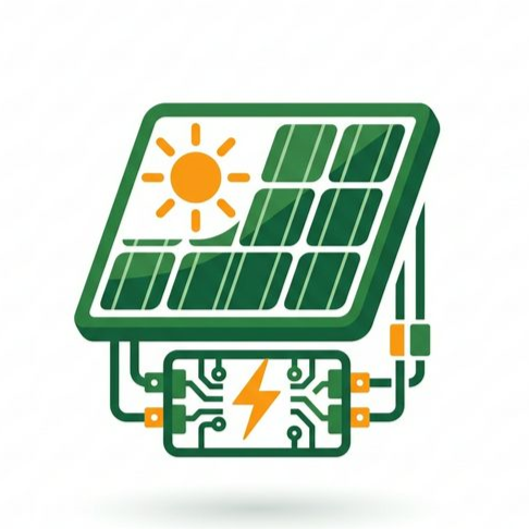
Solar PV inverters, MPPT charge controllers, Wind energy converters, Grid tie systems, Three-phase power conversion, EMI/EMC aware designs
Learn More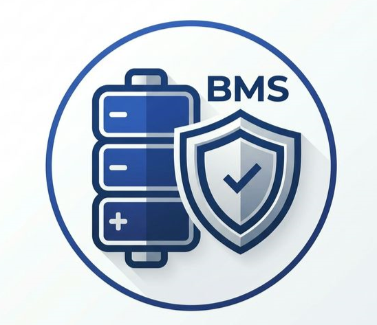
High voltage BMS up to 96S, Cell voltage monitoring, Active cell balancing, Overcurrent and overtemperature protection, HV isolation design, CAN bus interface
Learn More
Bidirectional DC-DC converters, Dual Active Bridge (DAB), Vienna rectifier, Isolated flyback and forward converters, Industrial SMPS, GaN and SiC based designs
Learn MoreOur core technical delivery framework — ensuring absolute engineering integrity from the first schematic capture to production-grade deliverables
Full system schematic capture — all sub-circuits documented in Altium Designer
Production-ready PCB layout — DFM compliant, thermally managed, EMI conscious
Complete end-to-end — schematic capture through to production-ready PCB in one engagement
Full design report — calculations, BOM, compliance notes, test plan
Design review, audit, technical advice — independent expert assessment
Complete end-to-end design — schematic capture through to production-ready PCB — delivered under one roof. Only senior engineers with full system knowledge can offer this. Most PCB layout services cannot.
Circuit Brilliance is built to be more than a design service — it is a growing power electronics design hub, bringing together deep engineering expertise, structured processes, and real-world project experience to serve the global EV and renewable energy community.
Beyond great PCB design — a structured, professional, and reliable engineering partnership
Documented, structured, repeatable process — every project, every time
Remote engineering delivery to EV and renewable energy companies globally
Schematic to production-ready PCB — single point of accountability throughout
Verified before fabrication — every time. Click here to know more
Engineering Assurance Frameworks
International Design Standards
PCB and System Level Thermal Verification
Across Four Domains

What five Ansys Maxwell 2D FEA simulations across 2-layer to 6-layer PCB winding geometries, spanning EQ30-class to E...
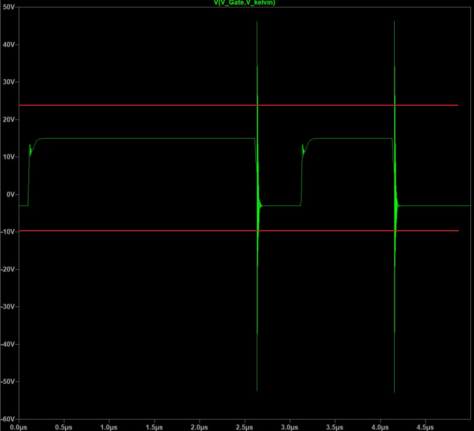
What a stiff current source reveals about gate loop vulnerability — and the critical damping threshold that protects ...
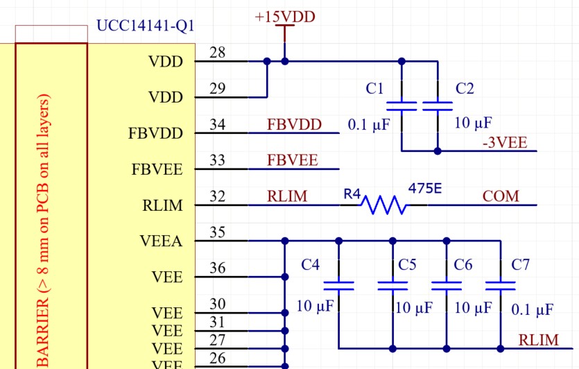
10 Field-Proven Best Practices for UCC14141 and UCC21755 SiC Gate Driver DesignThe UCC14141 and UCC21755 are excellen...
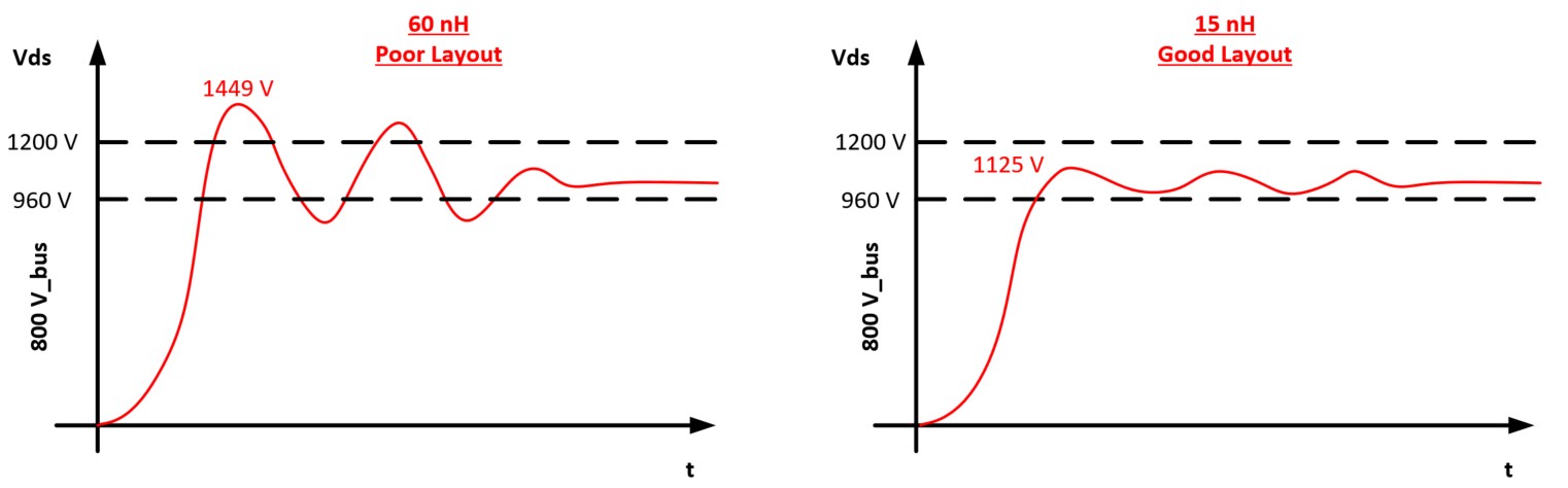
A SiC MOSFET fails at 900 volts. Its datasheet rating is 1200 volts. The gate drive is correct. The thermal managemen...
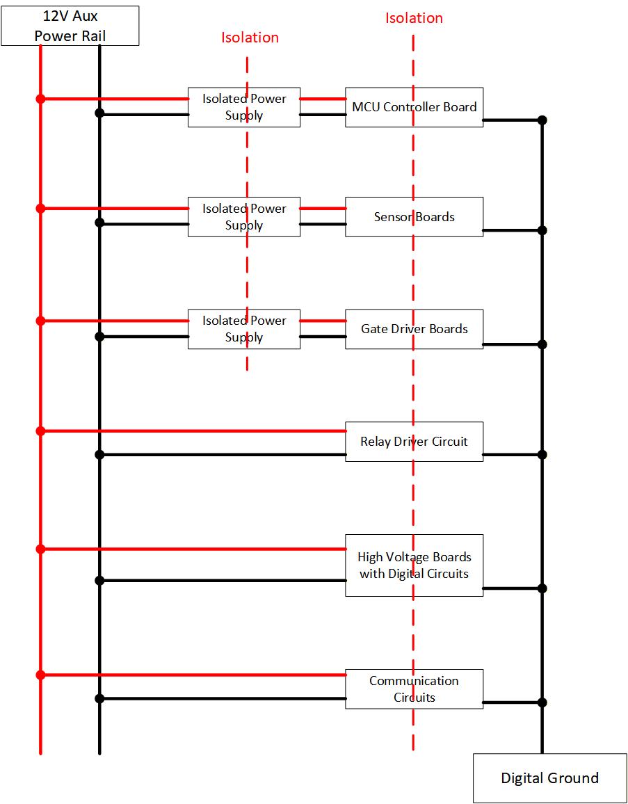
In SiC gate driver design, the most damaging grounding mistakes are also the most invisible ones. They survive schema...
The specialist search that keeps failing A new project lands on your desk. The internal team is already underwat...