
 Design
Leakage Inductance in Planar Transformers — What the 1D Formula Gets Right and Where It Falls Short
I compared the standard 1D analytical formula for planar transformer leakage inductance against Ansys Maxwell 2D FEA simulations across five PCB winding geometries.
Read Full Insight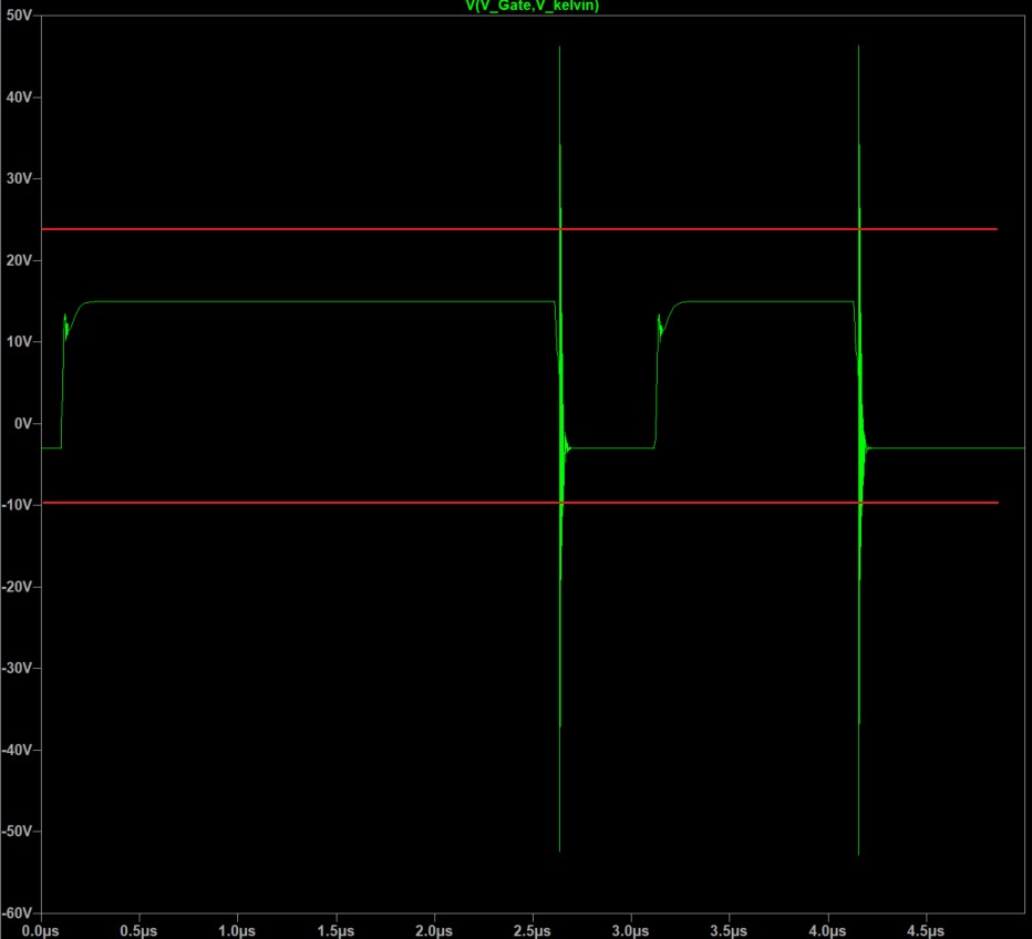 Perspectives
Replicating Physical PCB Parasitics in a 1200V SiC Double Pulse Test — An LTSpice Observational Study
A 1200V SiC Double Pulse Test replicated in LTSpice reveals two phases of gate-loop behaviour — unmitigated oscillation at +45V/−55V, and complete suppression above the critical damping threshold of 7
Read Full Insight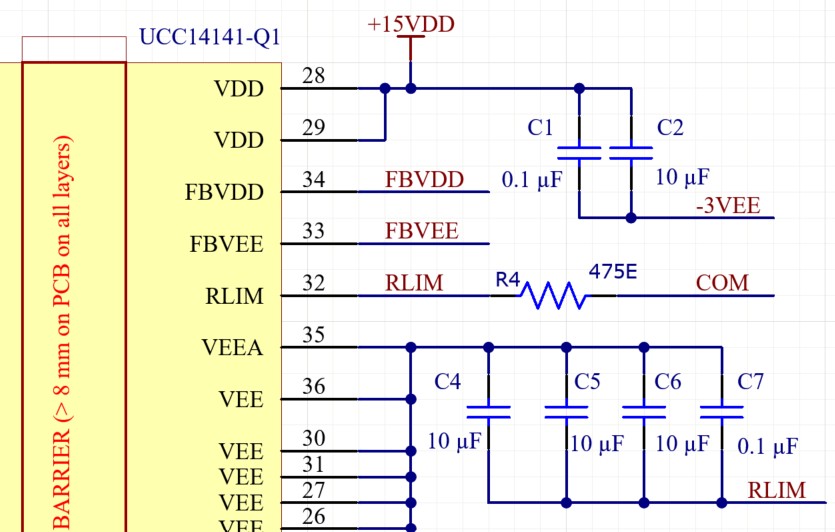 Perspectives
Why UCC21755 Gate Driver Works in Simulation but Misbehaves on the Bench
Ten field-proven best practices for the UCC14141 isolated bias power module and UCC21755 SiC gate driver — covering MLCC derating, decoupling hierarchy, PWM signal integrity, gate loop minimisation.
Read Full Insight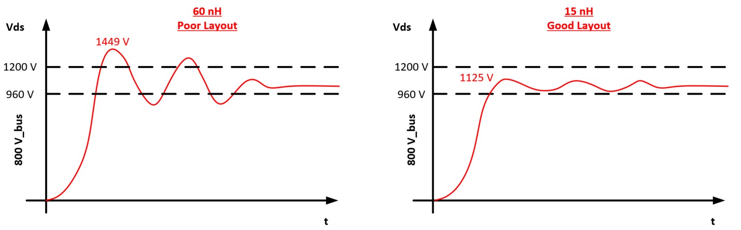 Perspectives
Why Does Parasitic Loop Inductance Destroy SiC Switching Performance?
Parasitic loop inductance is invisible on the schematic and lethal in a SiC circuit. What it is, where it hides in your PCB, and why V = L × dI/dt is the equation that decides whether your SiC device.
Read Full Insight