What a stiff current source reveals about gate loop vulnerability — and the critical damping threshold that protects a SiC gate oxide.
The semiconductor manufacturer's Double Pulse Test fixture is engineered for one purpose: to characterise the baseline switching performance of a raw silicon die in isolation. The PCB inductance is minimised by design. The parasitics are suppressed by construction. The result is a clean switching waveform that tells you what the device can do — not what your layout will do to it.
The system-level Double Pulse Test is a different instrument entirely. It keeps the device in place and changes everything around it. The bus voltage is real. The load current is real. The PCB layout is real — with its stray inductances, its shared return paths, and its geometric decisions made weeks earlier on a schematic that showed none of them. The system-level DPT runs the device for a cumulative window of a few microseconds at full application voltage and current density. It is the only non-destructive way to know whether the layout your team approved will destroy the device it was designed to drive.
This post documents an LTSpice observational study of a system-level DPT for a 1200V SiC MOSFET — the Navitas G3F75MT12J — at 800V bus voltage and 22A load current. The simulation replicates three physical PCB parasitics in a virtual layout mesh and observes two distinct phases of gate-loop behaviour: the unmitigated failure and the structured recovery.
This post is the sixth in the Circuit Brilliance series. If you have not yet read Post 4 on parasitic loop inductance and the V = L × dI/dt framework, that post provides the analytical foundation that makes this observational study readable.
System-Level DPT — What It Is and What It Is Not
A Double Pulse Test applies two gate pulses to a power switching device with a defined load current and bus voltage. The first pulse establishes the load current in the freewheeling inductor. At the end of the first pulse, the device turns off and the freewheeling diode commutates the current. The second pulse turns the device back on against the established load current — creating a full hard-switching turn-on event at the pre-charged bus voltage.
The semiconductor manufacturer uses DPT on a minimised fixture to characterise Eon, Eoff, and switching loss as functions of current, voltage, and gate resistance. Every parasitic in that fixture is deliberately minimised. The result is a datasheet number that represents the device's best-case switching performance.
The system-level design firm uses DPT for the opposite purpose — to stress-test the actual PCB layout before it is committed to full continuous-conduction operation. The PCB is not a minimised fixture. It is a real board with real routing decisions, real via placements, and real copper geometry. The stray inductances in that layout produce transient over-voltages and gate-loop disturbances that the device characterisation data cannot predict. A board that passes a static design review can fail catastrophically on its first power cycle. System-level DPT exposes this before it happens.
The governing principle of system-level DPT: Commencing continuous-conduction load testing on an unverified PCB prototype introduces immediate risk of catastrophic thermal failure from unforeseen layout resonances. System-level DPT resolves this risk by subjecting the physical layout to full application voltages and current densities for a cumulative window of only a few microseconds — safely exposing layout-induced transient over-voltages and gate-loop vulnerabilities before the hardware is committed to full-scale operation. |
Simulation Configuration — The Virtual Layout Mesh
The simulation network is configured to decouple the power-stage dynamics from external components. An 800V DC bus supplies an ideal constant current source locked at 22A — the nominal continuous current rating of the G3F75MT12J. Deploying an ideal current source instead of a discrete inductor model eliminates the parallel parasitic capacitances (EPC) and series resistances (EPR) of a real inductor, ensuring that all observed high-frequency behaviour originates strictly from the PCB layout parasitics under study.
Three parasitic parameters replicate the physical layout in the simulation mesh:
- L_int = 15 nH — models the physical gate trace routing length and the board-to-board vertical header pins bridging the driver card to the power substrate
- L_s = 15 nH — models the shared, non-Kelvinised copper return segment where both the high-current power loop and the low-current gate driver loop physically overlap
- C1 = 1 nF — a discrete stabilising capacitor placed immediately adjacent to the physical gate-source pins of the semiconductor package
The complete simulation parameters:
| Parameter | Value | Notes |
|---|---|---|
| DC Bus Voltage | 800 V | Represents automotive HV battery pack |
| Load Current | 22 A | Nominal continuous current rating of G3F75MT12J |
| Load Model | Ideal current source | Eliminates EPC/EPR — isolates PCB layout behaviour |
| L_int — Interconnect | 15 nH | Gate trace + board-to-board header pins |
| L_s — Common Source | 15 nH | Shared non-Kelvini-sed source return copper |
| C1 — Gate-Source Cap | 1 nF | Discrete stabilising capacitor at gate-source pins |
| Max Solver Timestep | 100 ps | Forces sub-nanosecond resolution — prevents numerical smoothing |
| Simulation Duration | 5 µs | Two complete gate pulses per run |
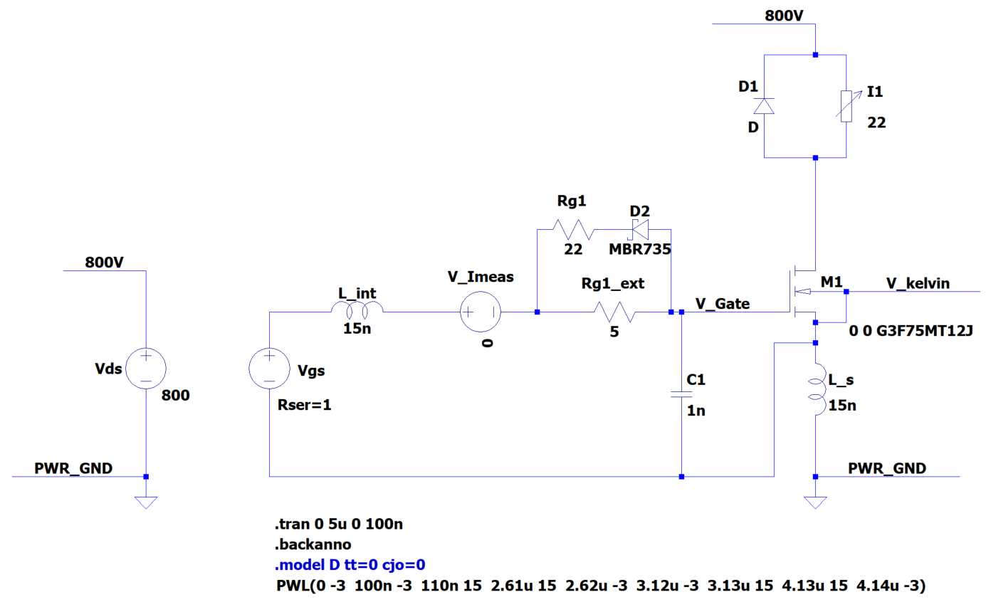
Figure 1 — Complete simulation schematic showing the 800V bus, ideal 22A current source, gate driver PWL source, three parasitic parameters (L_int, L_s, C1), and the G3F75MT12J MOSFET model.
Solver Constraint — Why 100 Picoseconds Matters
Standard adaptive time-stepping algorithms expand the calculation step to several nanoseconds during flat voltage intervals. At these step sizes, the ultra-high-frequency layout oscillations that occur at the instant the SiC channel breaks conduction — oscillations above 100 MHz generated by the interaction between layout inductances and localised capacitances — are numerically invisible. The solver integrates over them and reports a smooth waveform that does not exist in the physical circuit.
Forcing a strict 100-picosecond maximum step interval compels the matrix solver to compute the sub-nanosecond transient domain. The directive is a single line:
.tran 0 5u 0 100p This directive constrains the maximum timestep to 100ps regardless of how flat the voltage appears between steps. Without it, the sub-nanosecond gate ringing that the layout produces is smoothed out of existence by the adaptive solver before it can be observed. |
Phase I — The Shared Source Path Vulnerability
In the first phase of the analysis, the external gate-source capacitor C1 is omitted. The gate circuit is evaluated with only the external gate resistance Rg1_ext = 5.1Ω and the three layout parasitics.
When the PWL gate pulse initiates a turn-off transition, the G3F75MT12J channel cuts off the 22A current path in nanoseconds. This generates an extreme rate of current change — dI/dt — in the power loop. Because the power return loop and the gate driver return loop pass through the same localised copper trace, the shared common-source inductance L_s = 15nH converts this rapid current collapse into an inductive voltage spike across the shared segment:
| V_Ls = L_s × dI/dt |
This voltage bounce dynamically shifts the internal source potential of the MOSFET relative to the driver's ground reference. The common-mode power-stage transient is converted directly into a differential-mode voltage stress across the gate oxide — forcing the gate terminal into a violent, under-damped oscillation.
Phase I simulation result: Gate voltage V(V_Gate, V_kelvin) peaks at +45V and plunges to −55V. The absolute maximum transient gate-source ratings for commercial Gen-3 SiC dies are +22V / −10V. The simulated gate swing exceeds both limits by factors of 2× and 5.5× respectively. This is not a marginal exceedance. On a real board with this layout geometry, irreversible gate oxide rupture is the expected outcome. |
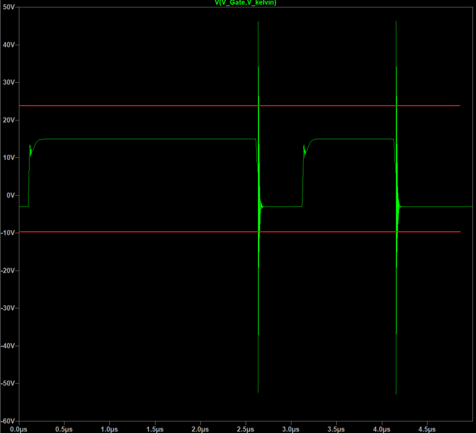
Figure 2 — V(V_Gate, V_kelvin) from Phase I simulation without C1
The mechanism is worth understanding precisely — because it is not the interconnect inductance L_int that produces this result. It is L_s. The interconnect inductance delays and distorts the gate signal. The common-source inductance converts the switching event itself into a gate-oxide stress. These are distinct failure mechanisms that require distinct layout responses.
L_int is fought by placing the gate resistor correctly relative to the interconnect. L_s is fought only by Kelvin source routing — physically separating the gate return path from the power return path so they never share the same copper. A non-Kelvinised layout with L_s = 15nH is not a marginal design choice. It is a device-destruction mechanism waiting for full operating voltage.
Phase II — Structural Over-Damping via Localised Capacitance
In the second phase, the layout is modified to include the 1nF external gate-source capacitor C1 placed immediately adjacent to the gate-source pins, combined with an increased external gate resistance of 10Ω.
The Critical Damping Calculation
The gate loop — L_s in series with the parallel combination of C1 and the device input capacitance Ciss — forms a second-order LC system. Whether this system rings destructively or settles cleanly is determined by one criterion: the total loop resistance relative to the critical damping threshold.
R_crit = 2 × √(L_s / C1) = 2 × √(15nH / 1nF) = 2 × 3.873 = 7.75 Ω Total loop resistance in Phase II: Rg1_ext + Rg_int = 10Ω + 1Ω = 11Ω 11Ω > 7.75Ω — the loop is mathematically overdamped. |
In an overdamped second-order system, there is no resonant frequency. There are no oscillations. The system transitions from one state to another along a monotonic trajectory — rising or falling without overshoot. The energy injected by L_s during the switching transient is absorbed by the resistive damping before it can build into an oscillation. The gate oxide sees only the intended drive voltage.
The Invariance Observation — The Post's Central Finding
Upon executing the transient solver at the 100-picosecond step size, a profound and practically significant behaviour emerges: the gate-source voltage waveform V(V_Gate, V_kelvin) is identical — to measurement precision — regardless of whether the 10Ω gate resistor is placed before or after the 15nH interconnect inductance L_int.
This invariance is not an approximation. It is a direct consequence of the overdamped condition. Once the total loop resistance exceeds R_crit, the system cannot sustain oscillation regardless of the internal arrangement of its components along an unbranched series path. The energy stored in L_int is completely absorbed by the 11Ω resistance before it can reflect back as a voltage stress on the gate oxide.
The Governing Observation
In an overdamped gate loop, the gate resistor position relative to the interconnect inductance is irrelevant. The question is not where the resistor sits. The question is whether the total loop resistance clears the critical damping threshold. Above R_crit, position becomes a secondary concern. Below it, position is the difference between a working design and a destroyed gate oxide.
The gate-source voltage in Phase II settles cleanly at the nominal +15V / −3V operating boundaries. The Miller plateau is clearly defined. The switching transitions are controlled and repeatable. The device operates within its ratings on every pulse.
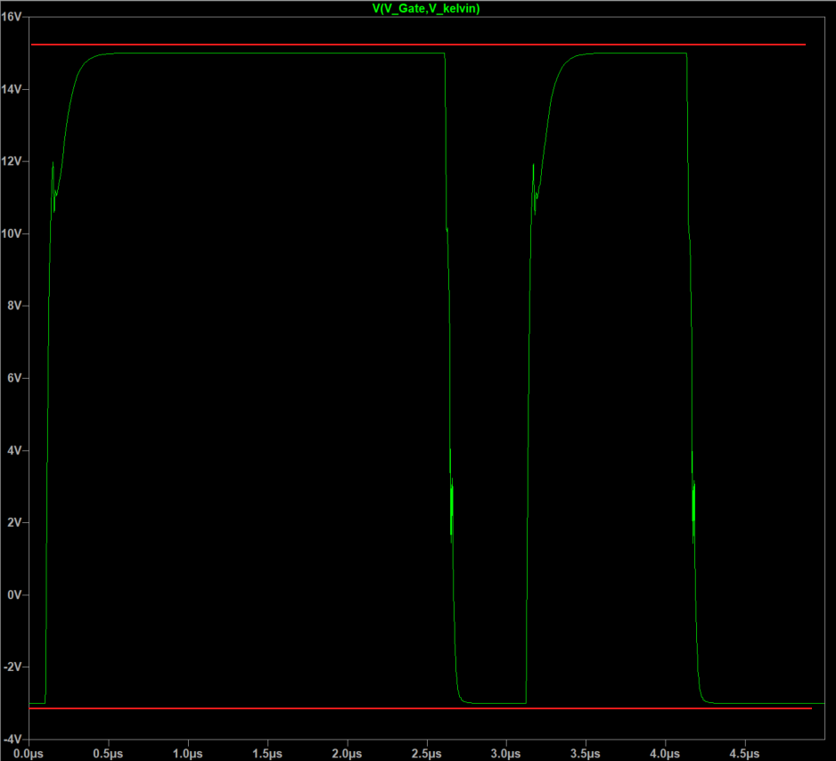
Figure 3 — V(V_Gate, V_kelvin) from Phase II simulation with C1=1nF and Rg=10Ω.
PCB Layout Takeaways
Three explicit design protocols emerge from this simulation study for high-speed power electronics boards operating with SiC devices above 600V.
1. Kelvin Source Routing Is Not Optional
The Phase I result is produced entirely by L_s — the shared common-source inductance. This inductance exists whenever the gate driver return current and the power stage return current share any segment of copper between the MOSFET source pin and their respective ground references. In a TO-263-7 SMT package with a dedicated Kelvin source pin, this sharing is eliminated by connecting the gate driver ground exclusively to the Kelvin pin and never allowing it to merge with the power source copper. Where a Kelvin source pin is unavailable, the gate return trace must connect to the source pad at the package boundary and be physically separated from the power source polygon immediately at that connection point.
2. The Capacitive Shunt Is a Structural Protocol
Where common-source inductance cannot be physically reduced below the threshold at which R_crit becomes achievable with practical gate resistance values, integrating a local gate-source capacitive shunt — C0G ceramic, 1nF to 4.7nF, placed directly at the gate-source pins of the semiconductor package — is a mandatory structural element of the gate drive design. It is not a tuning component. It is not an optional improvement. It is the element that makes overdamping achievable at gate resistance values that do not unacceptably increase switching losses.
3. The Overdamped Condition Eliminates Component Sequencing as a Layout Concern
The invariance result resolves a recurring debate in SiC gate driver PCB design: does the gate resistor position relative to the board-to-board interconnect inductance matter? The simulation provides a quantitative answer. It matters below R_crit. It does not matter above it. For any stacked gate driver and power module assembly where the total gate loop resistance — external gate resistor plus internal MOSFET gate resistance plus gate driver output impedance — exceeds the critical damping threshold calculated from the interconnect inductance and the gate-source capacitance, the debate is settled. Design for the overdamped condition and the position question becomes irrelevant.
Summary
| Takeaway | What It Means for Your Layout |
|---|---|
| Shared source inductance is the primary threat | L_s couples switching transients directly into the gate loop. Kelvin source routing is the structural solution. |
| Unmitigated gate voltage can exceed ±50V | +45V / −55V swing in Phase I far exceeds the ±22V / ±10V absolute maximum ratings of Gen-3 SiC dies. |
| R_crit = 7.75Ω is the design threshold | Total gate loop resistance must exceed this value to achieve overdamped operation with L_s = 15nH and C1 = 1nF. |
| Overdamped loops are position-invariant | Above R_crit, gate resistor position relative to L_int has no measurable effect on the waveform. |
| Local gate-source capacitance is mandatory | 1 nF C0G at gate-source pins provides the capacitive shunt that enables overdamping at practical resistance values. |
| DPT validates layout before full power | A few microseconds at full voltage exposes layout hazards before the first continuous-conduction test. |
The simulation does not end the conversation about gate driver layout in stacked SiC assemblies. It frames it. The conversation that matters is not about resistor position. It is about whether the total loop resistance clears the critical damping threshold — and whether the Kelvin source path is physically separated from the power return before the first pulse is ever applied.